MCU Design
The MCU has 4 roles in this project:
- Reading frames from the image sensor using its internal ADC
- Processing the frames (Debayering & Color Correction)
- Sending frames to the FPGA for compression
- Sending compressed frames to the computer for display via USART
These roles can be seen in the block diagram below:
MCU Block Diagram
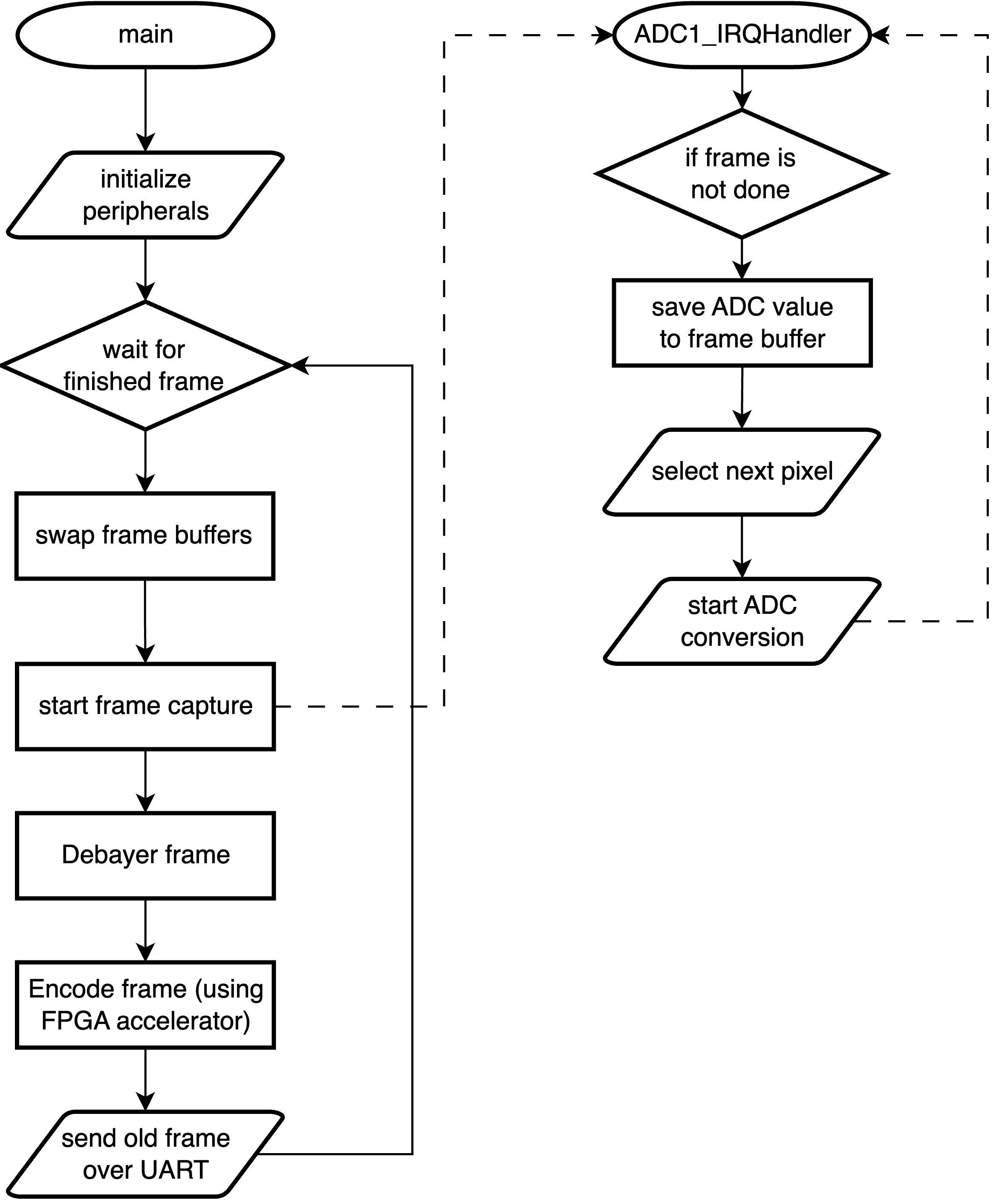
There are two main processes on the MCU: the main loop and the ADC interrupt handler. On boot up, the main loop initialized all the necessary peripherals (ADC, USART, SPI, and the FPGA). It also sets up two buffers for storing frame data in. Finally, it start the first ADC conversion (which will trigger the ADC interrupt handler, shown as a dotted arrow in the diagram).
Main Loop
In the infinite loop the MCU waits for the current frame to be finished. As soon as the frame is finished it swaps the frame buffers and tells the ADC to start capturing the next frame. While that is happening it debayers the image to go from greyscale to full color and sends it to the FPGA for compression (this is blocking rather than being done with interrupts). When the FPGA responds with the compressed image the MCU sends it over USART to be displayed on the laptop (see Python Script).
ADC Interrupt Handler
Each time the ADC interrupt handler is triggered it saves the current pixel into the active frame buffer. If it is not on the last pixel, it configures the analog muxes to select the next pixel and starts a new conversion. If it is on the last pixel, it sets a flag to tell the main loop that the current frame is done.
ADC Peripheral
The ADC is setup to read the voltage output of a single pixel on one of its 16 external channels. We are using the ADC at its maximum resolution of 12 bits and maximum sampling rate of 5.33 Msps (Note: the ADC sampling rate is not the limiting factor in our FPS, see results for more details). Nonetheless, the ADC is driven using the system clock at the maximum speed of 80 MHz to reduce sampling time as much as possible. We are using the ADC in left aligned mode with offset disabled so that the magnitude of the output does not depend on the ADC resolution.
There are several ways to start an ADC conversion (single conversion mode, continuous conversion mode, and hardware or software triggers). We chose to use software triggers to start all of our conversions because we want the highest possible sampling speed but also need to change the state of the analog muxes between each sample. As shown in the MCU Block Diagram, conversions are started in software from the main loop (at the beginning of a new frame) or in the ADC Handler Interrupt after the muxes have been setup for the next pixel.
Interfacing with Image Sensor
There are 3 components to interfacing with the MCU, row selection, column selection, and output.
Row selection uses a 32:1 analog mux that is built into the sensor PCB. There are 30 rows so 5 address bits are required to select the necessary row.
Originally, we planned to use 3x 16 channel external ADCs and read from all columns at once, however we scaled down the design to be more achieveable in the timeline of this project (that would have required a 3rd custom PCB that we didn’t have time to create). Because of that change, we opted to use three 16:1 analog muxes (CD74HC4067) on our breadboard to control the 40 columns. Using three 16:1 muxes instead of one 64:1 mux requires slightly more complicated addressing logic than for the row selection. The MCU outputs a 6 bit signal indicating which column it wants to select. The lower 4 bits are wired to all three 16:1 muxes while the upper 2 bits are wired to a 2:4 bit decoder on the FPGA that controls the enable pin on each of the three 16:1 muxes, only activating the correct one based on the column the MCU wants to select.
All of the address selection is done using the GPIO pins on the MCU.
ADC Peripheral and ADC Interrupt Handler have more details on exact process of setting up the ADC and reading individual pixels. Below is a trace of the voltage input to the ADC while one whole frame was being captured.
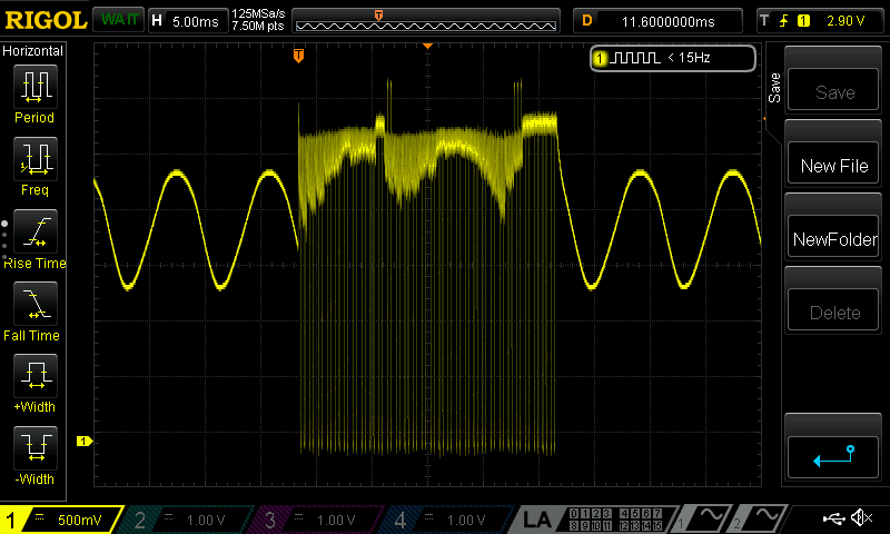
Sensor Oscilloscope Trace
Note that the ~120 Hz component of the signal is due to the flicker of the fluorescent lights in the digital lab.
Image Processing
The output of the image processing pipeline is a 8 bit 30x40 QOI encoded image. We chose to use the ADC in 12 bit mode even though the final image is 8 bit to prevent color banding and other image artifacts caused by insufficient color resolution.
Image Processing Pipeline
Color Correction
The brightness and contrast of the image straight from the camera sensor depend on a lot of factors including: the ambient light and the resistor used in the phototransistor circuit.
To correct the brightness and contrast, we use alpha-beta adjustment as described by Richard Szeliski in Computer Vision: Algorithms and Applications, 2nd ed.
The pixel \(f(i,j)\) in the input image is adjusted using the following equation:
\[g(i,j) = \alpha \cdot f(i,j) + \beta\]We set \(\alpha = 1.1, \beta = -0.1\) to create an image had a reasonable amount of contrast and black level close to 0.
Debayering
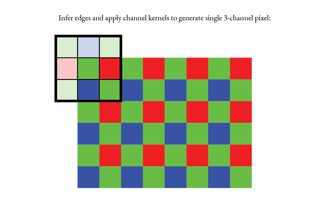
A physical Bayer filter covers the camera. The pixel locations determine the “color” of each value.
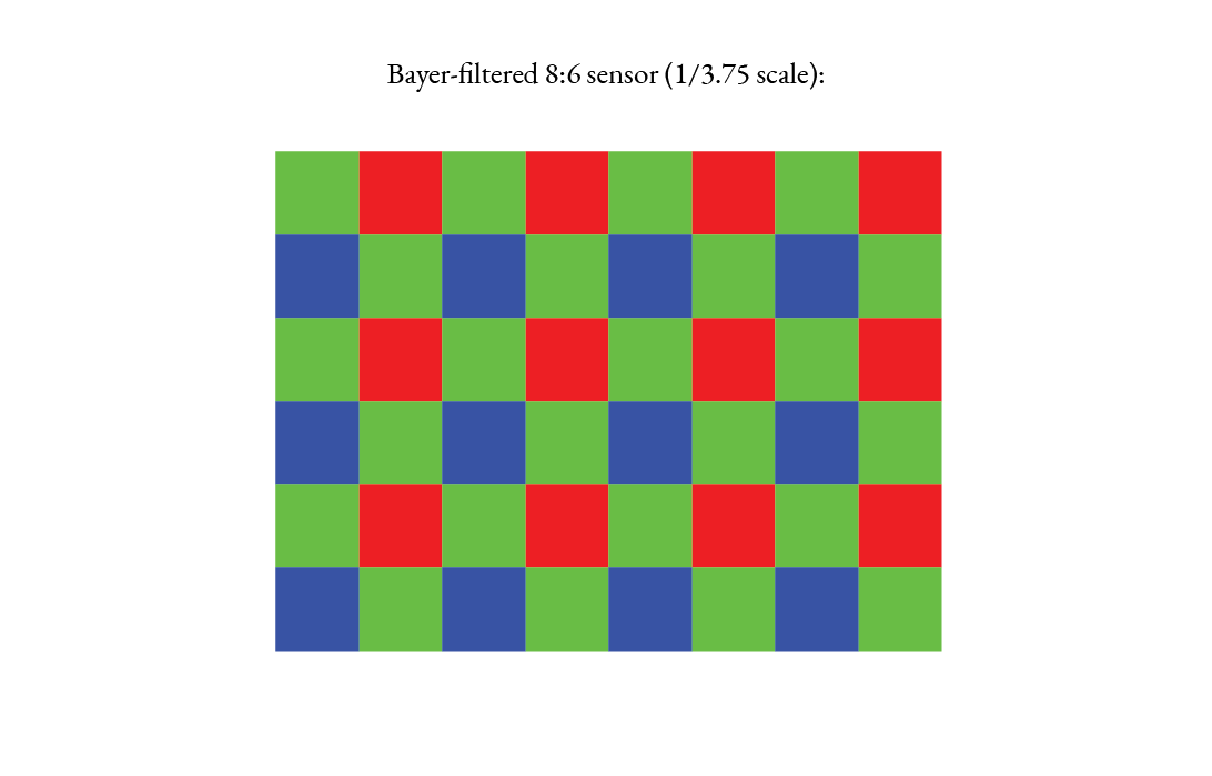
The filter is applied to the sensor, and we obtain a single channel image

Debayering is the process of converting this single channel image (visualized below in grayscale) into an image with full color per each pixel.
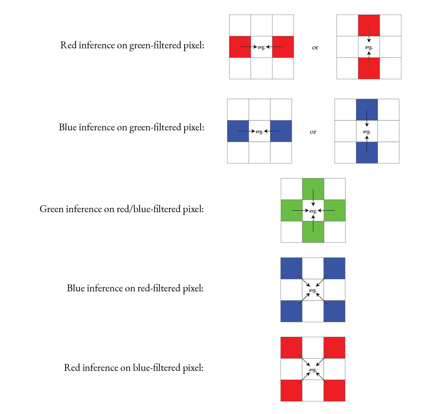
Each color channel of each color pixel is calculated as a linear interpolation of adjacent values of the respective color.
Each color pixel can therefore be obtained from the values of the 3x3 grid of single-channel values centered on its location.
This 3x3 grid covers out-of-bounds values when calculating pixels on the border of the image.
Naively, one would extend the border pixels as necessary to fill the filter input. This violates the Bayer patern, which may instead be preserved by copying/mirroring the row/column one removed from the edge. Pixels on two edges (i.e. corner pixels) are accounted for by sequentially mirroring horizontally/vertically, where the ordering making no difference. Pre-handling the (literal) edge cases enables the 3x3 kernel logic to remain simple.
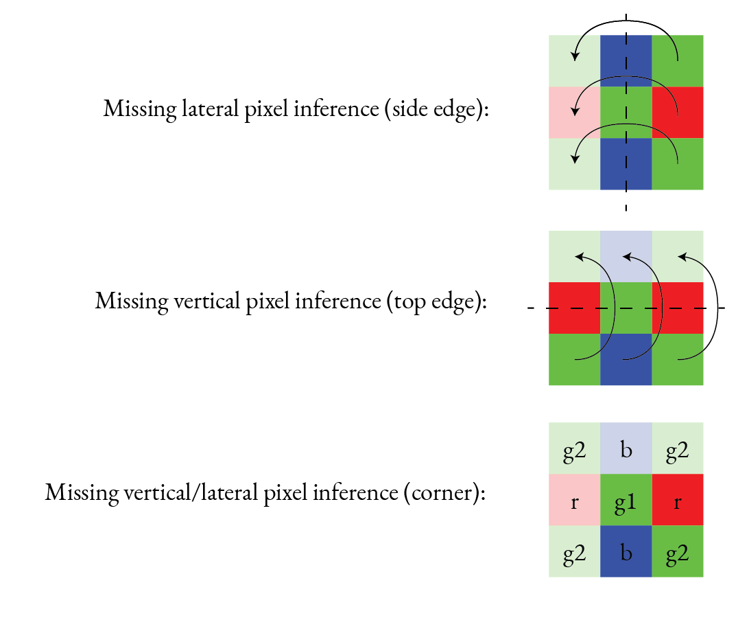
This edge-handling diagram extends rotationally to all other edges and corners.
It would be theoretically ideal that in the case of a green corner, the diagonally inferred pixel would be sampled from the corner itself rather than the green pixel one removed from both edges.
This ends up not mattering as the 3x3 kernel samples channels directly on the same color tile, so the green channel of the green corner Bayer tile corner is sampled directly anyways, irrespective of what green pixels are mirrored.
We proceed to shift the 3x3 kernel to be centered at all the coordinates of the image until the full color image is calculated.
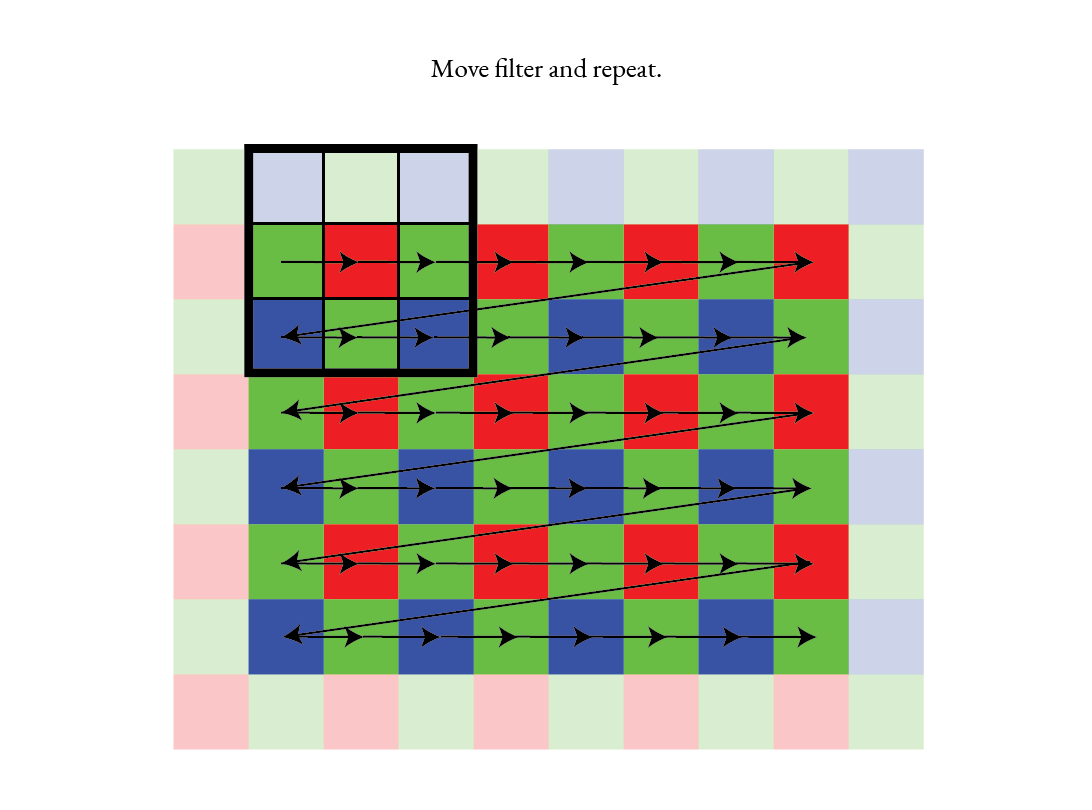
The final result looks as follows.

Compression & SPI Peripheral
The MCU and FPGA communicate using over SPI using a custom sequence of commands as shown below:
until response is not
0x80 or 0x081 end F-->>M: Send compressed image Note right of M: Continue reading
until last 8 bytes
match footer
Compression Sequence Diagram
The SPI peripheral is setup with a 5 MHz clock with polarity of 0 and phase of 1. There is only one device on the SPI Bus (the FPGA) so the chip select line is replaced with a reset signal for initalizing the compression algorithm each time before use.
The full reset sequence involves:
- Raising the reset line
- Writing 0xAF twice
- Lowering the reset line
See FPGA Design for a detailed explanation of how compression is implemented.
USART Peripheral
The primary goal for this project is to build a functioning camera not to drive a display, so we chose USART as simple protocol for sending images to a laptop.
After the image is captured, color corrected, debayered, and compressed, it is converted to hex and sent over USART to the laptop. We chose specifically to use USART_2, which transmits through the built in Micro-USB port on the Nucleo board for simplicity. We are transitting with a baudrate of 921,600 which was the highest we could go without running into signal integrity issues and dropping a significant number of frames.
See results for more information the maximum frame rate we were able to achieve.
Python Script
To display images from the camera we wrote a python script that reads the serial output from the MCU and displays the images in a window. The script can be found in our github repository here. The script uses the PySerial library to read the serial output, OpenCV to display the images, and qoi to decode the images.
It supports reading QOI compressed images, or raw color or greyscale images (all of which can be selected with command line arguments). The script also supports displaying the images in a window and saving them to a file.